Case study: 8 and 14-layer HDI with Stacked Vias
This case study focuses on the challenges and solutions that we implemented to design complex HDI boards with stacked vias.
Case study: 8 and 14-layer HDI with Stacked Vias

An in-depth analysis on PCB stackup – PCB HERO

How to allow microvia between two inner layers? - Layout - KiCad.info Forums

Standard PCB Thickness: The Ultimate Guide for You in 2022
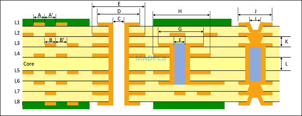
Staggered Microvias and Stacked Microvias PCB in HDI PCB

High-Speed PCB Design- Layer Stack-Up, Material Selection, and Via Types, by Ca
HDI board stack-ups – PCB HERO

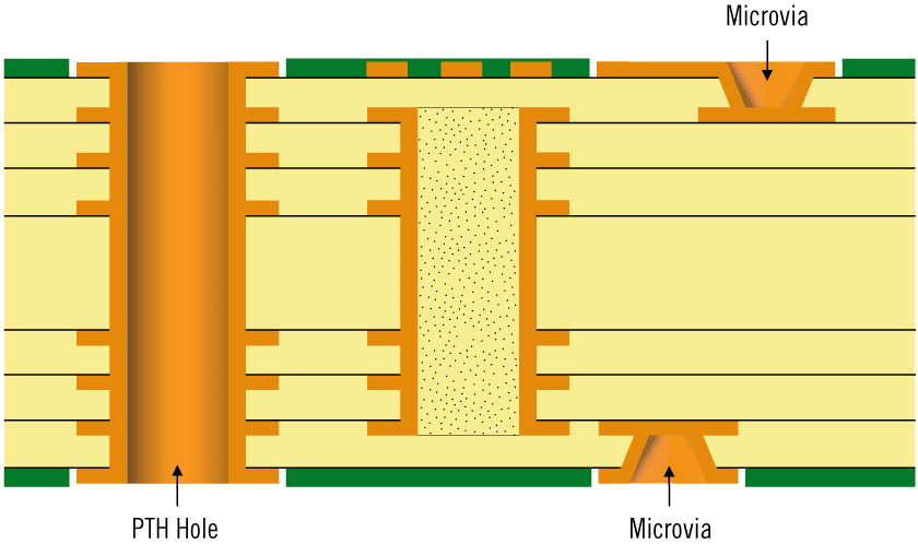
Understanding Proper PCB Design (Part 2) - Circuit Cellar

Ultimate HDI PCB Manufacturer in China PCBTok

Stacked and Staggered Via to Optimize PCB Design and Manufacturing

Understanding Proper PCB Design (Part 2) - Circuit Cellar
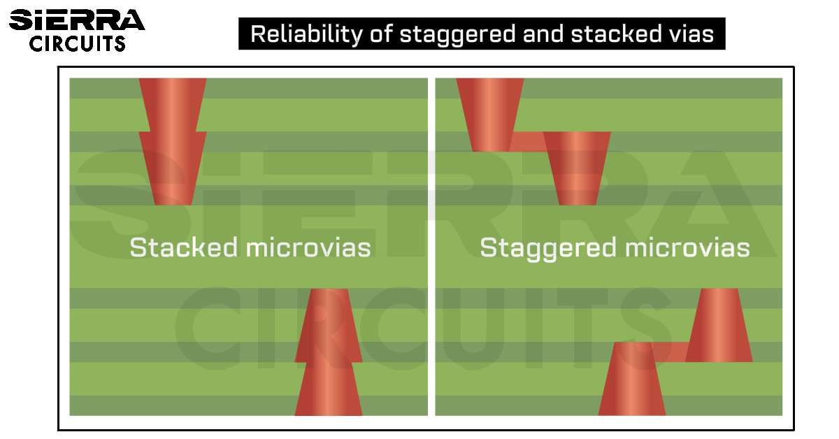
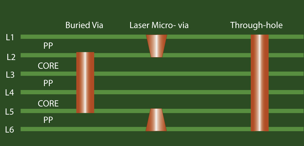
Designing Staggered and Stacked Vias
Different Stackups for HDI PCBs - Rush PCB