
Pocket implanted n-MOSFET structure with split drains.

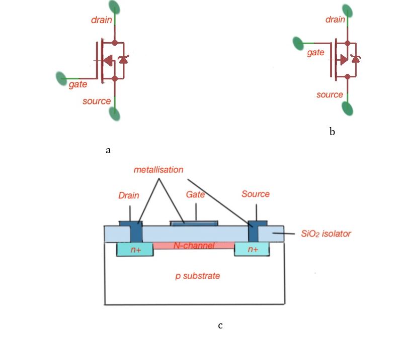
Planar MOSFETs and Their Application to IC Design
Semiconductor Devices: Depletion MOSFET
Planar MOSFETs and Their Application to IC Design

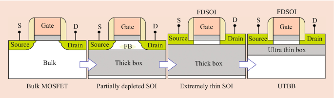
Sensors, Free Full-Text
Micromachines, Free Full-Text

Fabrication process flow of NiGe metal S/D CMOSFETs. P þ im

Asymmetric n-channel pocket implanted MOSFET.

Planar MOSFETs and Their Application to IC Design
Q.D.M. KHOSRU, Professor

FETs (Field-Effect Transistors) - Discrete Semiconductor Products - Electronic Component and Engineering Solution Forum - TechForum │ DigiKey
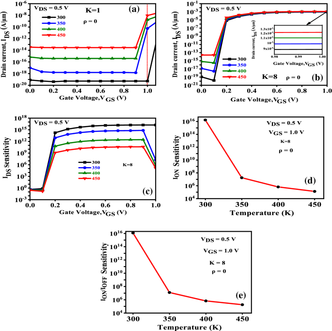
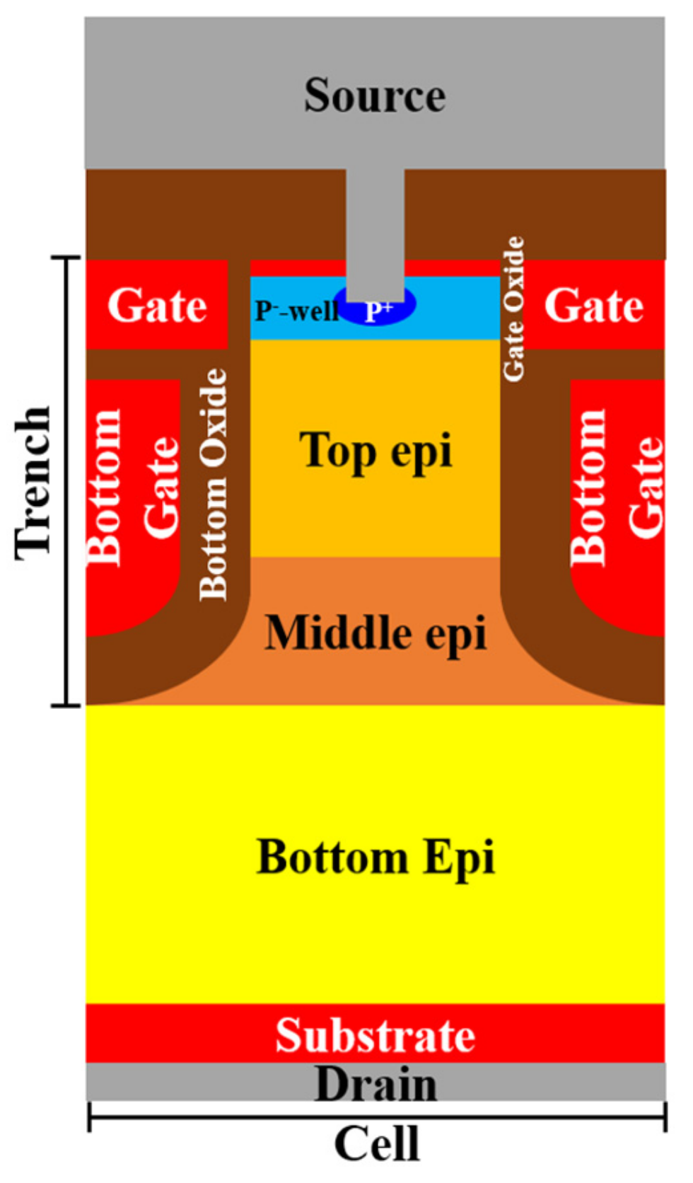
Performance assessment of cavity on source dual material split gate GaAs/InAs/Ge junctionless TFET for label-free detection of biomolecules

Electronics, Free Full-Text

A half micron MOSFET using double implanted LDD

Pocket implanted n-MOSFET structure with split drains.


:max_bytes(150000):strip_icc():focal(899x148:901x150)/SPIDER-MAN-INTO-THE-SPIDER-VERSE-110722-01-c5377dc1dc204aceb5e3d93e1327ecd0.jpg)
