Substrate-Like PCBs Push the Limits of HDI
5
(446)
Write Review
More
$ 16.00
In stock
Description
High-Density PCB Design Planning, Advanced PCB Design Blog
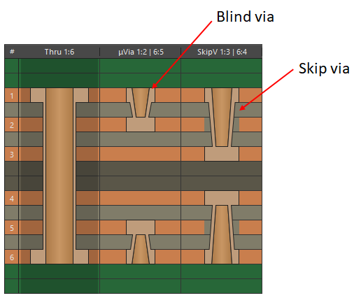
Blind And Buried Vias—What Are They And How Are They Used?, PCB Design Blog
PDF) Eight key HDI design principles

Blind And Buried Vias—What Are They And How Are They Used?, PCB Design Blog
Introduction to High Density Interconnection, HDI Design
Microvia Technology and Beyond for HDI Design, Blog
What is Ultra-Small Spacing Substrates?
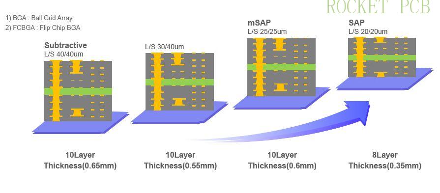
High-end Hdi Anylayer Mass Production Capacity-rocket Pcb
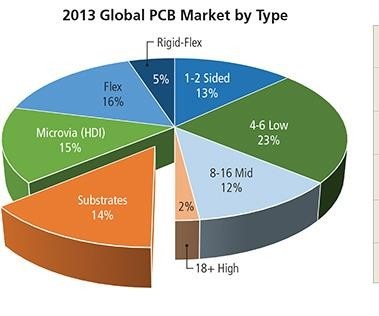
Printed circuit boards: A mobile market

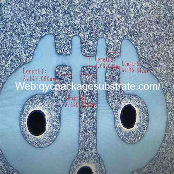
Substrate-like PCB shrinks conductor trackwidths to 15µm - EE Times Asia

PCB develops towards HDI - from single-layer to substrate-like PCB - IBE Electronics

HDI PCB Design and Manufacturing

Focus on Embedded Development for PCB Designers
Related products


You may also like