The outline of bump bond process steps. (1) deposition of field
4.7
(397)
Write Review
More
$ 8.99
In stock
Description

Literature Review Of Portfolio Management Essays
AFM Exclusive

15544557.ppt

The outline of bump bond process steps. (1) deposition of field metal

Development of electrodeposited multilayer coatings: A review of fabrication, microstructure, properties and applications - ScienceDirect

Left) X-ray image of a line pair rule taken using an un-collimated
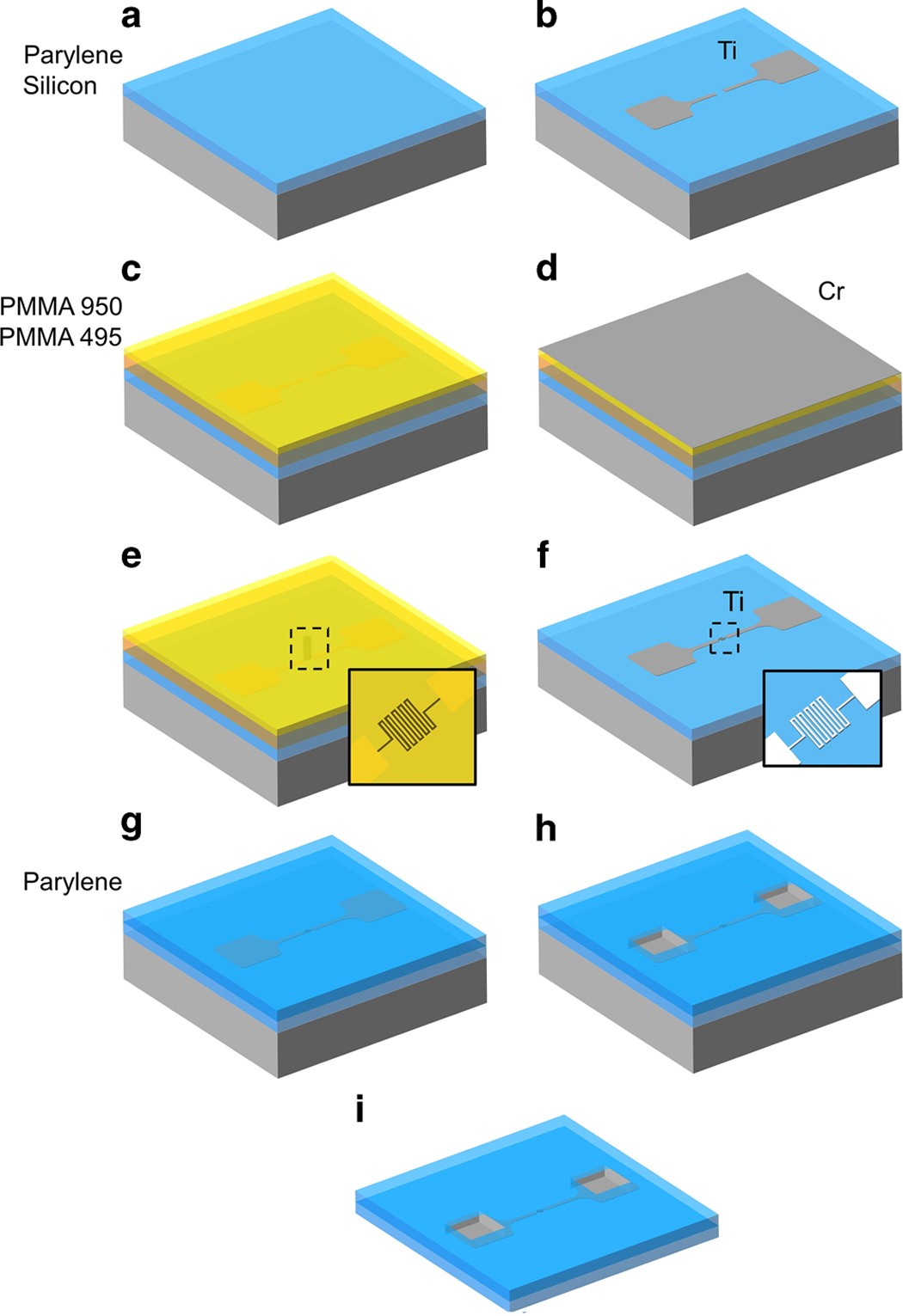
Electron-beam lithography for polymer bioMEMS with submicron features
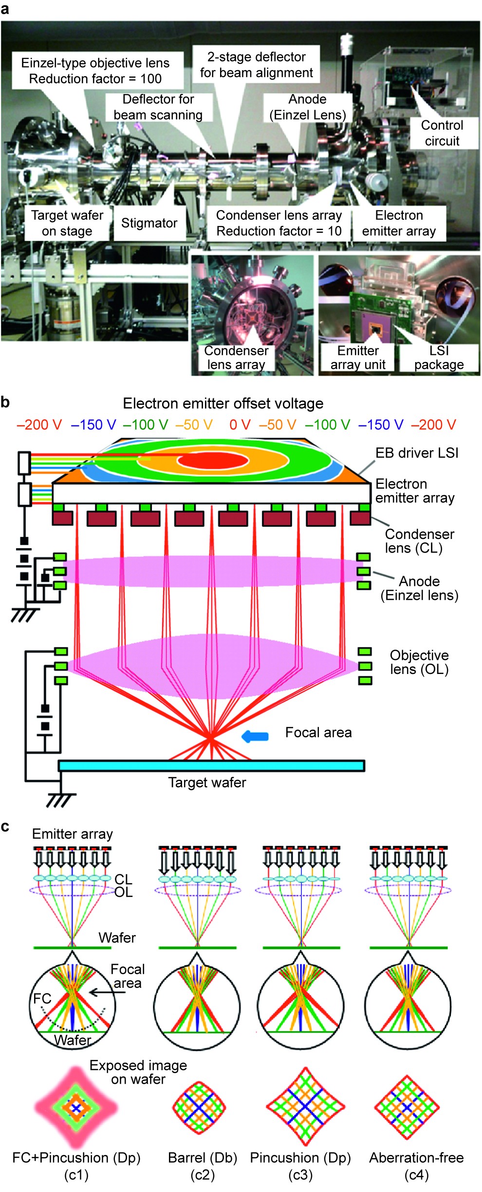
Development of massively parallel electron beam direct write lithography using active-matrix nanocrystalline-silicon electron emitter arrays

A. Peacock's research works European Space Agency, Paris (ESA) and other places

Hans ANDERSSON, Principal Research Engineer

Schematic drawing of the bonding process with different temperature
Related products

:fill(ffffff)/http%3A%2F%2Fstatic.theiconic.com.au%2Fp%2Fbonds-6956-3611102-1.jpg)


You may also like