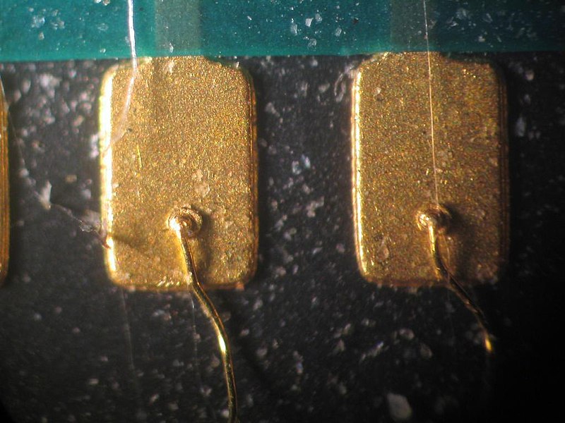
What is a Pad in PCB Design and Development
4.9
(738)
Write Review
More
$ 22.99
In stock
Description
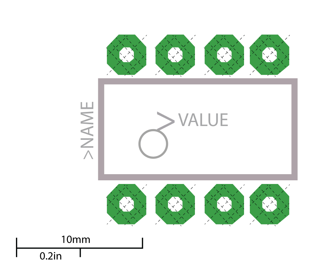
A pad is critical to PCB design as it serves as the designated surface area for electrical contact between the component and the board.

PCB Fab Express on LinkedIn: RAPID PROTOTYPE SERVICE
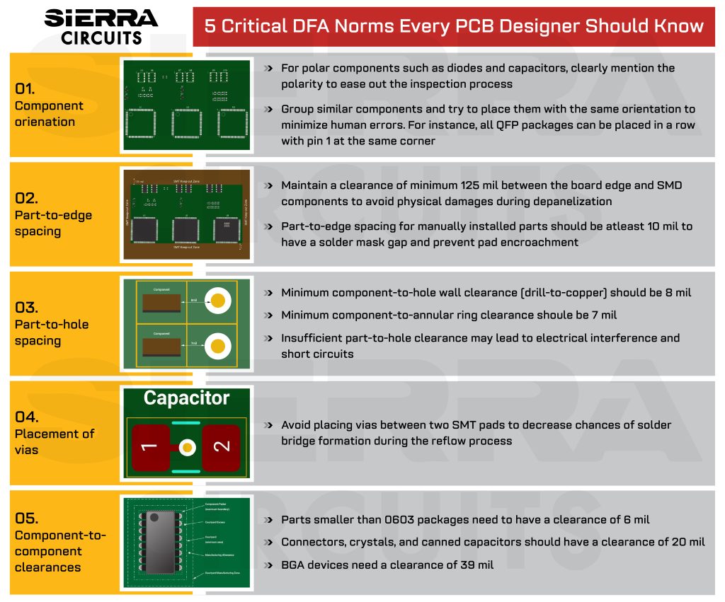
14 Tips For PCB Design For Assembly
接触焊点- 维基百科,自由的百科全书
Component Placement in PCB Design & Assembly
What is a Pad in PCB Design and Development
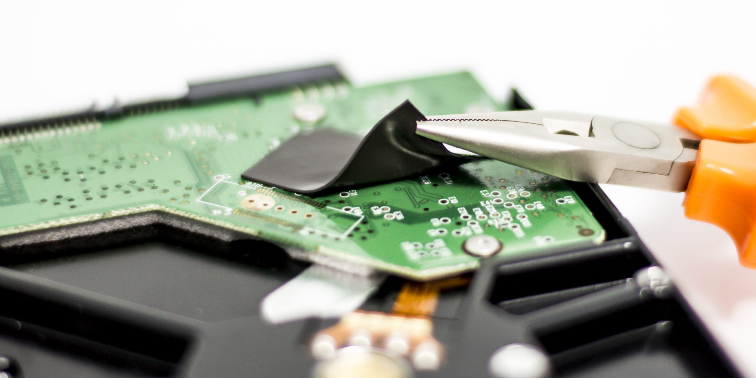
Thermal Pads in PCB Design & Manufacturing

What is Thermal Relief in PCB during the PCB Manufacturing Process

PCB Basic Knowledge_84
What is a Pad in PCB Design and Development

What is a Pad in PCB Design and Development
PCB Basic Knowledge_84
PCB Basic Knowledge_84
PCB Basic Knowledge_100

What is a Pad in PCB Design and Development? - Absolute
Related products


:max_bytes(150000):strip_icc()/Best-Chemical-Peel-Pads-For-Effortlessly-Glowy-Skin-tout-116c14e0cfdd40f08eb29ae36d91e3ee.jpg)