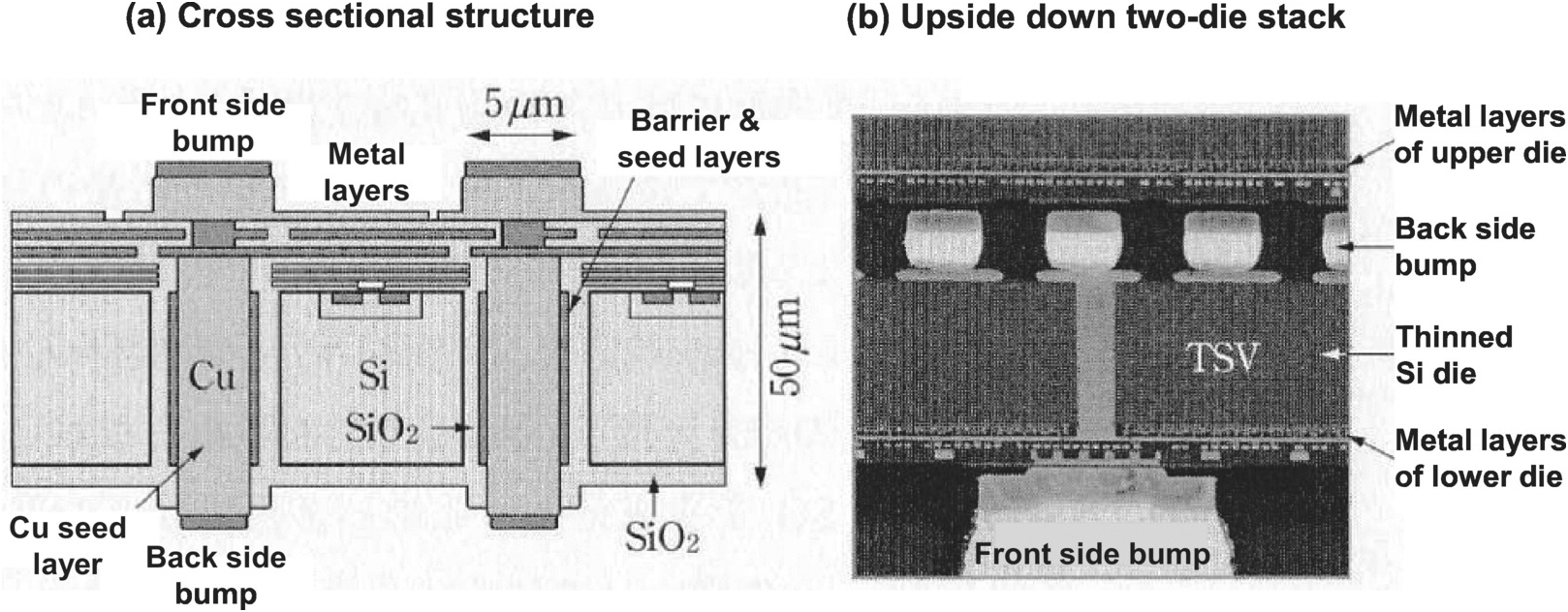
Schematic of the chip/bump build-up cross-section.

Semiconductor Back-end Process 3: Packages

Wafer Cross-Sections Through the Bumping Process

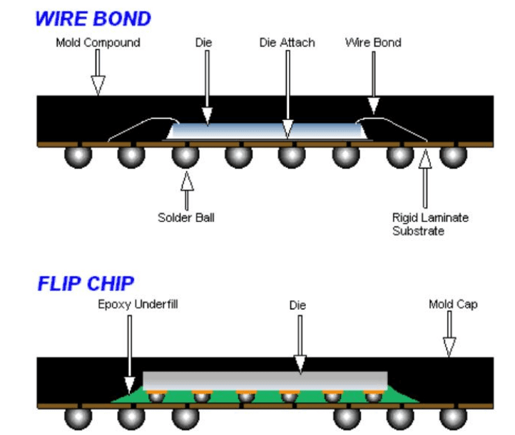
Cross-section of FCPBGA and enlarged cross-section of flip chip

Zhuojie WU Research profile

Challenges Grow For Creating Smaller Bumps For Flip Chips
What Are Through-Silicon Vias?
GIS Dictionary

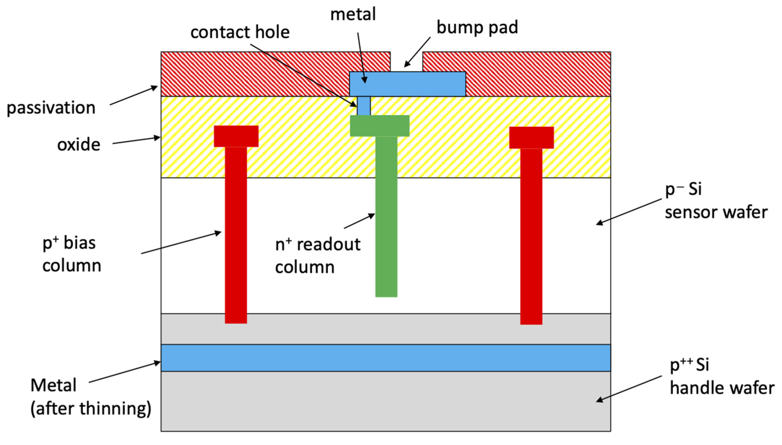
Developing an accurate and robust tool for pixel module
Introduction (Chapter 1) - Wireless Interface Technologies for 3D

Challenges Grow For Creating Smaller Bumps For Flip Chips

PDF) Understanding and Improving Reliability for Wafer Level Chip
Weibull plots for TCoB fails based 1000 ohms and 0.1 ohms
Flip-Chip BGA: PCB Layout Best Practices - Free Online PCB CAD Library
pub.mdpi-res.com/chips/chips-02-00006/article_depl

PDF) Understanding and Improving Reliability for Wafer Level Chip