pcb - What is the pad size required for this BGA AW H3 Chip
I'm trying to figure out the pad size to use for my footprint according to this datasheet.The last page in the datasheet has the package dimensions. I've also posted the relevant information in a p

Repair damaged BGA chip pad

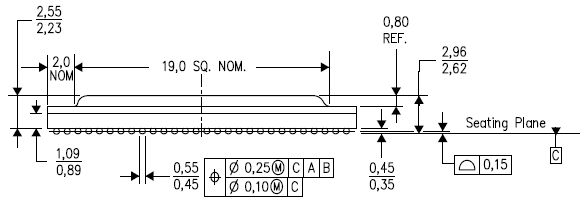
pcb - Question about a dimension in this IC package drawing - Electrical Engineering Stack Exchange
Top PCB Layout Recommendations for BGA Packages
TDA2SG: recommended pcb pad size of TDA2 bga - Processors forum - Processors - TI E2E support forums
Can I remove my 32GB eMMC and replace it with a 64GB SSD? - Quora
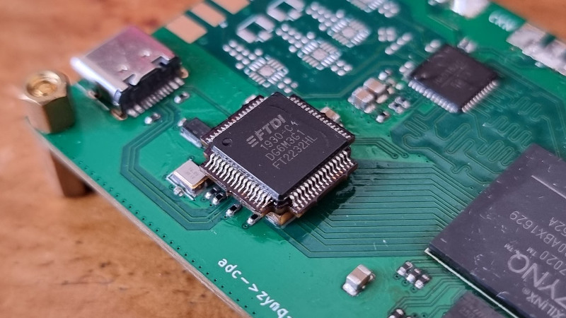
Nifty Chip Adapter Does The Impossible

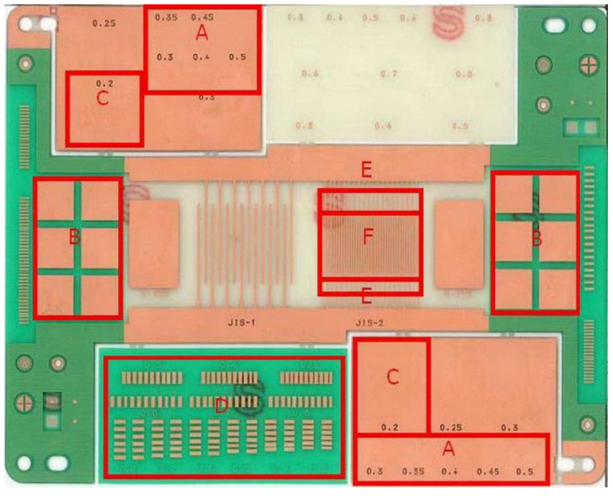
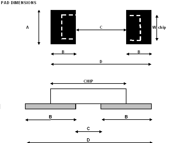
BGA Pad Size Deep Dive Component Creation

iW-RainboW-G50M i.MX 93 or i.MX 91 OSM-LF LGA Module Hardware User Guide
Materials, Free Full-Text
Pad Layout - Johanson Technology
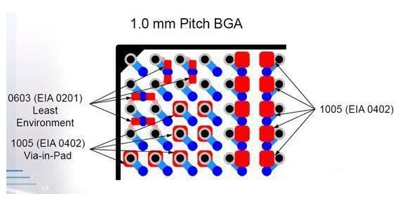
BGA pad design standard and basic rules

BGA Pad on a PCB - EEWeb
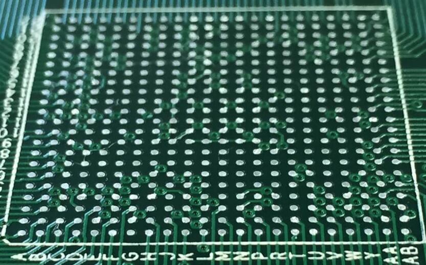
BGA pad design standard and basic rules
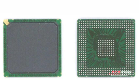
An Introduction to BGA by PCBGOGO
)