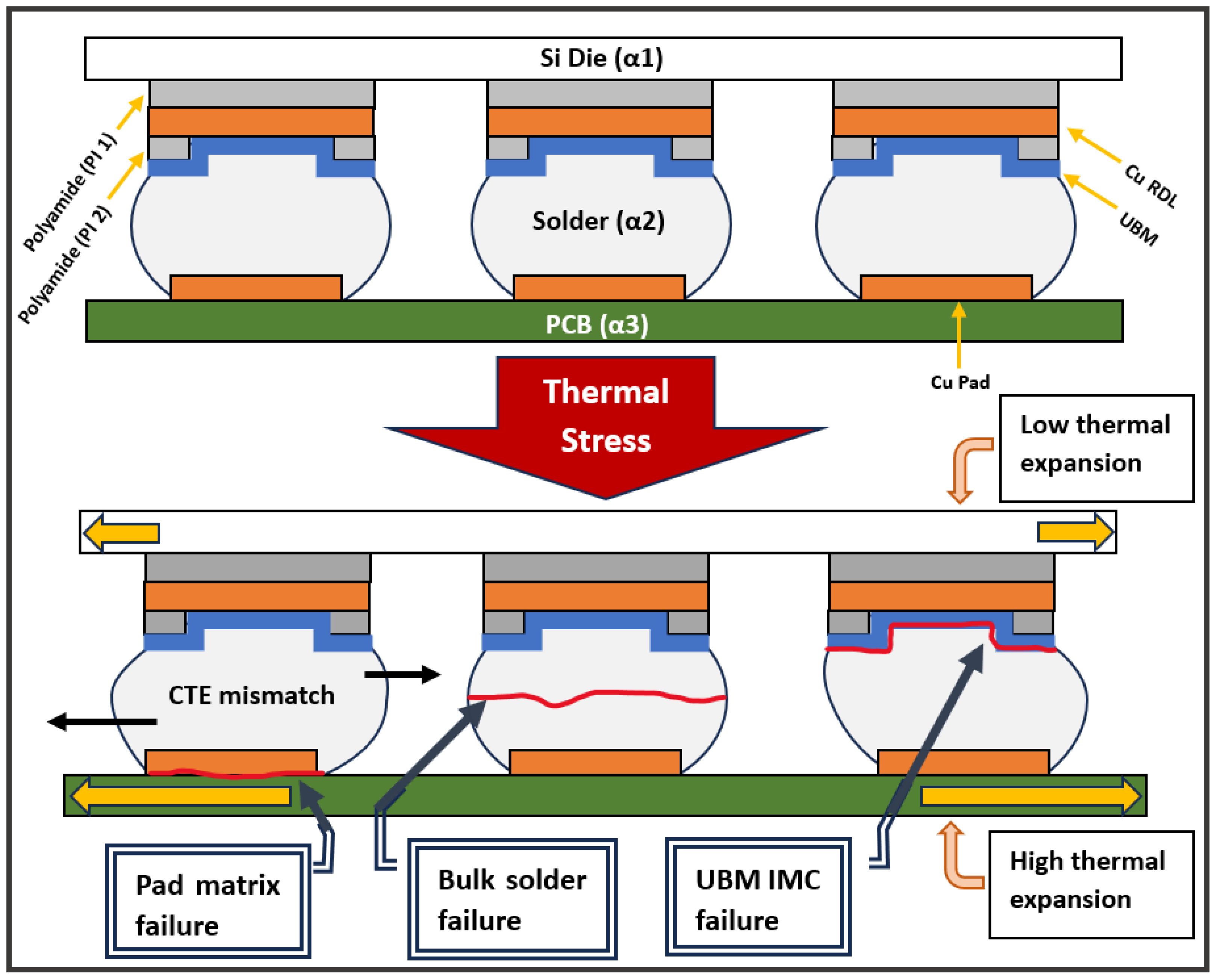
The bond pad redistribution layer (polyimide 1) and the under bump

US6660624B2 - Method for reducing fluorine induced defects on a

Warren FLACK, Vice President, PhD
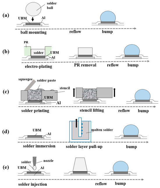
Materials, Free Full-Text

Illustration of polyimide or LCP substrate and solder assembly

Process integration of fine pitch Cu redistribution wiring and
_en.png)
redistribution layer (chip) (RDL)

Redistribution in wafer level chip size packaging technology for

PDF) Fan-Out Wafer-Level Packaging (FOWLP) of Large Chip with

Electromigration Performance Of Fine-Line Cu Redistribution Layer
Micromachines, Free Full-Text
PDF) Redistribution layers (RDLs) for 2.5D/3D IC integration

Process integration of fine pitch Cu redistribution wiring and

CN111108144A - Curable polyimide - Google Patents
Optimizing Chiplet Packaging for Complex Applications - QP

Warren FLACK, Vice President, PhD